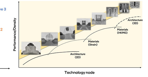
This paper examines the periodicity of innovation in the history of computing and attempts to predict what may be next. A multitude of innovations across many disparate disciplines were critical enablers in the relentless pursuit of Moore’s Law. These innovations evolved individually at their own pace over many years, if not decades, sometimes in fields entirely unrelated to semiconductor processing. Progress for each innovation experienced fits and starts and occurred without any set periodicity until it was adopted in high-volume semiconductor manufacturing.


As an example, Copper wires on a chip were enabled by the invention of the chemical-mechanical polishing (CMP) process in the 1980s and subsequent deployment by the semiconductor industry in the 1990s. The planarization process to make nanometer scale copper interconnects on silicon chips today is commonly referred to as the Damascene process.
Building more transistors and increasing on-chip transistor density was just one ingredient in realizing the promise of Moore’s Law. Equally important were innovations that enabled chip designers to effectively use the exponentially growing transistor counts to build increasingly complex circuits. And just as important were innovations that enabled architects to envision and build increasingly sophisticated and capable computers with the abundant transistors.
Accelerating Returns Built Upon Diminishing Returns
Innovations that exponentially increased transistor density; innovations that enabled designing with exponentially more transistors; innovations that enabled building more sophisticated computers; and innovations that enabled more user-friendly computing devices – all followed a similar evolutionary pattern. Progress in nearly every major innovation was defined by a characteristic S-curve with a long period of gestation, followed by rapidly accelerating progress and widespread adoption and finally, an extended period of evolutionary or incremental progress along a diminishing returns curve.
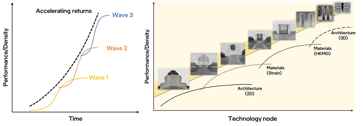
Every major shrink in transistor geometry was enabled by a combination of many innovations, each traversing a different point along its own diminishing returns curve. The aggregate of all these innovations delivered a near doubling of transistor density with every shrink. In other words, accelerating returns in transistor density were enabled by the aggregate of diminishing returns from many discrete innovations in materials science, engineering, solid-state device physics and many other disciplines.
Building More Transistors
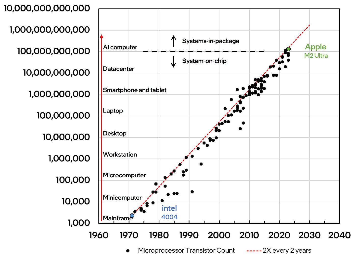
Some transistor geometries (aka nodes) were anchored around major process, material or architecture inflections (e.g. SiGe to introduce uniaxial strain in the transistor or the FinFET architecture to improve transistor electrostatics). When such changes were first introduced into volume manufacturing, they delivered substantial, step-function improvement along one or more specific vectors (e.g. higher drive current with strained silicon or lower leakage current with the FinFET) and with every subsequent geometry shrink, the innovation continued to be refined and improved until it reached a point of diminishing returns. For example, the FinFET architecture was refined over 5 geometries until it finally began to run out of steam. The next evolutionary architecture (RibbonFET) has already been in development for many years and will be ready to be introduced by the time the FinFET runs its course – and the cycle will then repeat. Not every transistor shrink required radical inflections in process technology and architecture. Several technology nodes were enabled purely by evolutionary improvements to build upon prior revolutionary changes. Rather than look for periodicity in transistor innovations over time or over geometry, it is instructive to look for periodicity over transistor counts. Since the microprocessor represents the most complex of semiconductor chips, it is a good proxy to use for such an exercise.

The added transistor counts occasionally led to smaller microprocessor die sizes, but often, they led to larger die sizes as architects found novel ways to add more functionality using the additional transistors. As an example, initially the microprocessor chip consisted of just a standalone central processing unit (CPU). Over time, it evolved to include more functional blocks (e.g. the floating point unit) and now consists of a highly complex and integrated system-on-a-chip (SoC) including the CPU, the graphics processing unit (GPU) and many other functional blocks including memory and IO circuits.
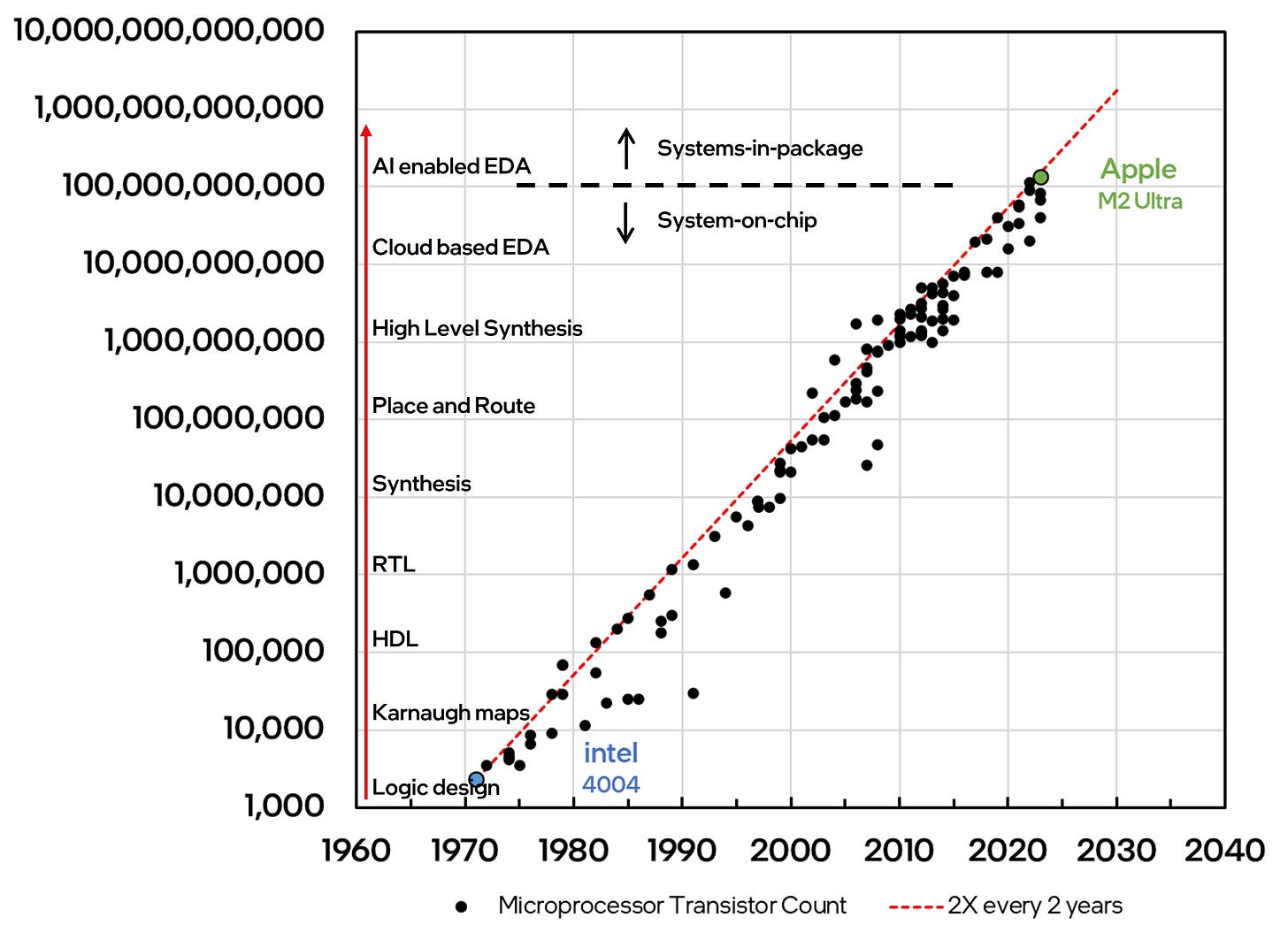
Transistor counts under 100 billion have generally been accommodated on a monolithic SoC. Transistor counts greater than 100 billion, while feasible on a single chip, are more likely to be accomplished via integration of multiple chips to build a system-in-a-package (SiP). Rather than innovations at the foundational transistor level, this next S-curve is likely to be at the system level, enabling architects to connect discrete digital logic, memory and analog chiplets with each other. Remarkably, this inflection from system-on-a-chip to systems-in-package was also envisioned by Gordon Moore in his seminal observation nearly 60 years ago:
“It may prove to be more economical to build large systems out of smaller functions, which are separately packaged and interconnected. The availability of large functions, combined with functional design and construction, should allow the manufacturer of large systems to design and construct a considerable variety of equipment both rapidly and economically.”
Gordon Moore, 1965 (from the original paper and prediction that became Moore’s Law)
Designing with More Transistors
Over time, engineers relied on computer-aided-design (CAD) tools to manage the growing complexity of chip design. This evolution was covered in Part 1 when discussing abstraction layers:
CAD evolved to become an industry in its own right and later came to be known as Electronic Design Automation (EDA). Here again, with every 10X increase in transistor count, there was at least one significant EDA innovation that progressively raised the level of abstraction and made it easier for designers to manage large and complex chip designs. Looking ahead, we are already seeing artificial intelligence (AI) driving the next major S-curve in EDA.
Creating Computers
With CAD enabling increasingly complex chip designs, architects were able to envisage and build more sophisticated microprocessors. All modern computers are based on the von Neumann architecture which introduced the concept of storing instructions and data in a shared memory. Astonishingly, this architecture was conceived in 1945, long before the invention of the transistor (1947), the integrated circuit (1958) or the advent of modern semiconductor processing (1960s) that would enable it to be brought to life in silicon.
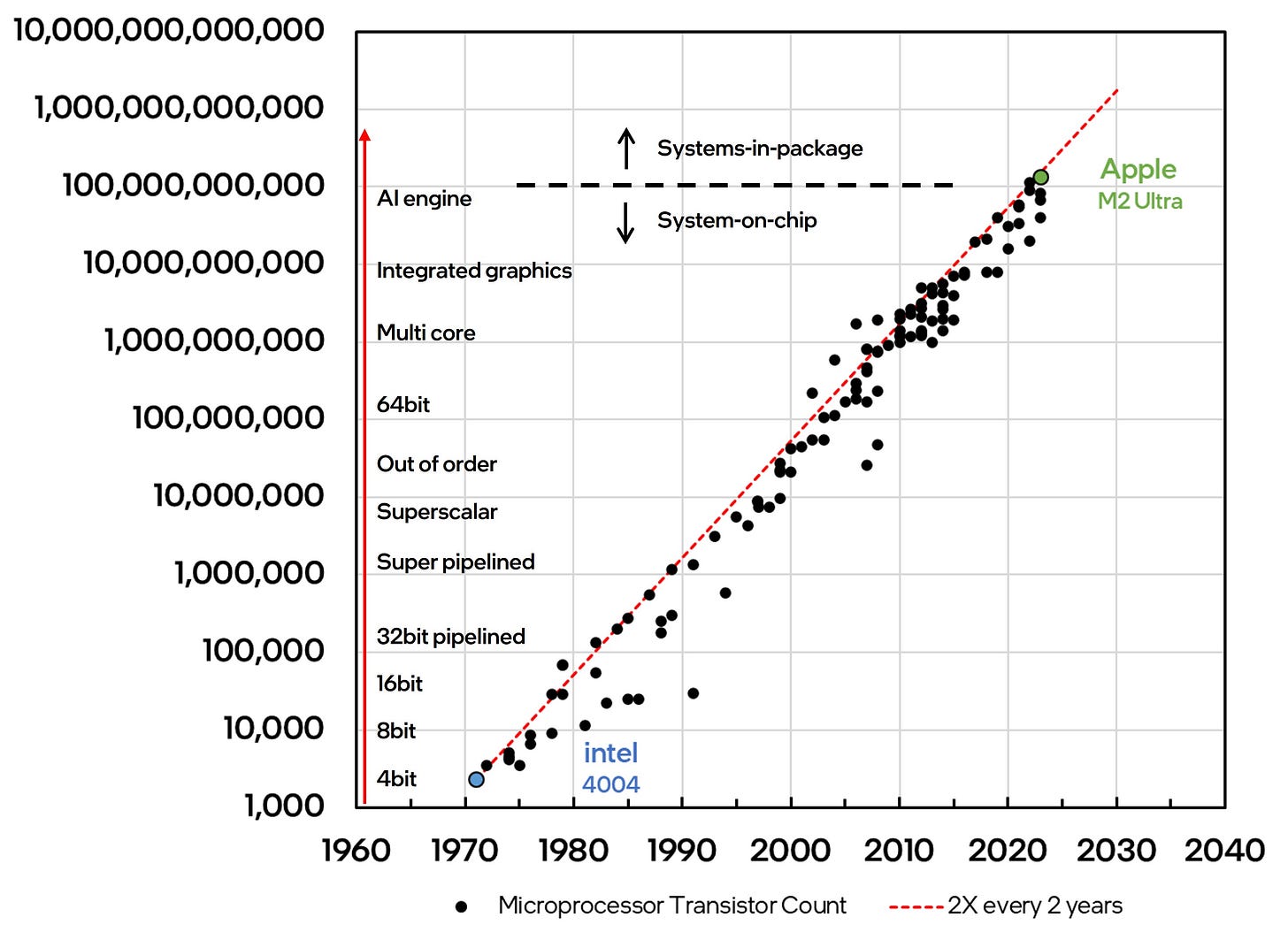
Starting with early innovations that included the addition of local cache memory, there have been numerous innovations in computer architecture that progressively took advantage of the exponentially growing transistor density. On average, every 10X increase in microprocessor transistor count enabled the introduction of a major innovation in computer architecture. Over time, progress in computer architecture came from three major ideas or S-curves – wider instruction widths (from 4-bit to 64-bit), instruction-level parallelism (from many cycles-per-instruction to many instructions-per-cycle) and core-level parallelism (from single-core to dual-core to many-core). Notable among these, instruction-level parallelism eventually led to two distinct architectural paradigms – “found” parallelism, commonly referred to as “out-of-order” processing which became the foundation of all modern CPUs and “given” or “explicit” parallelism which became the foundation of all modern GPUs. All this progress was enabled not only by increasingly abundant transistor counts, but also by increasing clock speeds (from a few Hz to a few GHz) with faster transistors.
In recent years, architectural innovation also included the incorporation of domain specific computing blocks (e.g. integrated graphics engines and neural engines). Looking ahead, computer architects will envisage new machines optimized from the ground up for machine learning and AI workloads. The next S-curve will also necessitate a new hardware-software contract for the computers of tomorrow.
Using Computers
Innovations in computer architecture drove the creation of increasingly sophisticated computing systems with progressively denser compute and storage capabilities and richer functionality. These innovations combined with a multitude of advances in hi-tech design, manufacturing and assembly enabled system and product architects to imagine and invent newer classes of computing devices in a variety of form factors from mainframes to smartphones. Here again, a periodicity with microprocessor transistor count is evident as a new class of computing emerged with every 10X increase in transistor count. The evolution of computer classes over time was first observed by Gordon Bell and is commonly referred to as Bell’s Law of Computer Classes.
What is Next?
Over the last 6 decades, innovations that enabled Moore’s Law facilitated the miniaturization of computing form-factors – from mainframes and workstations to the mobile computing devices of today. The silicon platforms that enabled these applications in turn became the primary drivers of continued innovation in process technology, design and architecture and defined the trajectory of the semiconductor industry for decades. As an example, the general-purpose CPU platform drove innovation during the PC wave of computing while the mobile Application Processor Unit (APU) platform drove innovation during the mobile wave of computing. Three broad trends are likely to drive the trajectory of transistor scaling and innovation in the semiconductor industry in the coming years:
First, diminishing returns in transistor density and increasing process cost will lead to diminishing improvements in cost per transistor. Many, if not most mass-market consumer electronics products may not be able to justify the increased cost and diminished returns on investment when scaling from one node to the next. This trend has already been evident for a few years. A decade after the introduction of the FinFET transistor, the last non-FinFET transistor process still commands the highest wafer volumes on par with the leading-edge node today. For the first time in 15 years, Apple now deploys the same mobile APU chip to power two consecutive annual iPhone models. Evolutionary improvements on mature technologies will continue for much longer than in the past as the cadence between revolutionary enhancements continues to lengthen.
Second, the ascendant AI wave of computing will favor highly parallelizable, tensor-based architectures as the primary computing engines in datacenters worldwide. These new architectures and platforms will displace the traditional general-purpose CPU and play an increasingly important role in driving innovation in transistor technology and more broadly in setting the trajectory of the semiconductor industry.
Finally, the datacenter itself is becoming a modular compute platform. High-performance computing systems are relatively more resilient to increasing wafer prices and hence more likely to serve as primary drivers of Moore’s Law in an era of flat or rising cost per transistor. Rather than drive a miniaturization of form factors, these high-performance computing applications require advanced packaging and system integration technologies to drive large-scale integration at package-, board- and rack-level. Innovation will be needed in a variety of areas including advanced logic, high-density memory, high bandwidth connectivity, thermal management and power delivery. The NVIDIA HGX100 module, Tesla Dojo and the Google TPU pod are examples of this trend – while they leverage advanced process technology to build individual compute, storage and networking chips within a module, it is the entire module or pod with tens of thousands of individual hardware components, along with supporting firmware and software APIs that forms an individual unit of computing. Merchant silicon providers that specialize in a discrete single-chip solution will be at a disadvantage over system and platform providers as the locus of innovation moves to holistic system integration technologies to enable the AI wave of computing.
The views expressed herein are the authors’ own.

