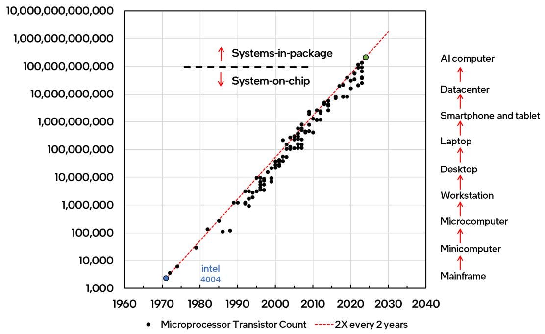
2025 will mark the 60th anniversary of Gordon Moore’s prescient observation that became the catalyst for silicon transistor scaling and the modern digital age.
We are on track to witness a remarkable milestone by the end of this decade – one trillion transistors within a tiny microprocessor package. This paper takes a sweeping view of waves of innovations that enabled transistor scaling over the last six decades and outlines critical innovations that will be necessary for continued transistor scaling over the next ten years.
Significant breakthroughs in materials engineering, device physics and process integration will be needed to overcome the most daunting challenge in computing today – lowering energy consumption to enable sustainable deployment of the exponentially growing demand for Artificial Intelligence (AI). Meeting this critical challenge will require the development of a revolutionary new transistor capable of operating at ultra-low supply voltages (lower than 300mV) while delivering acceptable performance (switching speed). This paper highlights the most promising future transistor options and envisions a transistor architecture that may meet these challenges.
Looking Back — Classical Scaling (CPU) Era: 1965 – 2005
The first four decades of Moore’s Law witnessed exponential growth in transistor count and enabled multiple successive eras of computing, starting with the mainframe and culminating with the Personal Computer (PC). Every 10X increase in transistor count enabled the creation of a new class of computers that built upon the prior generation.

Moore’s Law (1965) along with the scaling physics established by Bob Dennard (Link) in 1974 provided technologists a blueprint to steadily shrink transistor dimensions while also progressively increase transistor performance at relatively constant power density. This happy marriage between Moore’s Law and Dennard scaling ushered in a golden era of computing that spanned nearly 4 decades. This era was made possible by numerous innovations in semiconductor equipment technology, materials engineering and process integration, most important being the consistent reduction of gate dielectric thickness (Tox) and the development of progressively shallower source/drain (S/D) extensions which enabled scaling of transistor gate lengths from micron-scale to nanometer-scale while lowering transistor threshold voltage (Vt). This period required a significant reduction in transistor operating voltage (Vdd) from 5V (up to the early 1990s) to just 1.2V (around 2005) to maintain product reliability with progressively thinner gate dielectrics. These innovations enabled chip clock frequencies to increase from mere tens of kHz to an incredible 3GHz.

Over time, the quest for raw performance (switching frequency), especially in PC (CPU) chips, forced faster dimensional scaling compared to voltage (Vdd) scaling, thus increasing electric fields across the device. Furthermore, additional Vdd scaling became limited by increasing off-state leakage (Ioff). This led to progressively higher power densities and, eventually, the breakdown of Dennard scaling itself. Power density was pushed to ~150W/mm2, the limit allowed by the economics of packaging and thermal dissipation capabilities of the day. By 2005, the industry found itself facing fundamental barriers to continued transistor scaling.
Looking Back — Mobile (SoC) Era: 2005 – Present
During the last 20 years, technologists broke through multiple seemingly insurmountable barriers to transistor scaling, including perceived limits to dimensional scaling, limits to transistor performance, and limits to operating voltage reduction. This era marked the emergence of mobile computing, which shifted the focus of transistor development from chasing raw performance (switching frequency or clock speed) to maximizing performance within a fixed power envelope (performance-per-watt).
Nonetheless, exponential growth in transistor counts continued unabated, albeit without the tailwinds of Dennard scaling, thus presenting computer architects an entirely new challenge – how best to utilize an abundance of transistors to improve performance and functionality while staying within a fixed power budget. This constraint was addressed by an architectural solution – core-level parallelism. Many computing tasks could be sped up by parallelizing them across two or more computing cores while consuming less total power. This gave rise to the era of dual-core and later, multi-core microprocessors. Even with multi-core architectures, increasing power density would eventually render sizeable blocks of transistors unusable at any given time (also known as “dark silicon”).

Concurrently, the transistor reached physical limits of silicon dioxide gate dielectric thickness (Tox) scaling and a progressive degradation in silicon channel mobility became apparent, which threatened to limit further gains in performance and power efficiency.
Radical transistor innovations would become necessary to surmount these perceived fundamental barriers.
Seminal Transistor Innovations Led by Intel
Starting in the early 2000s, engineers at Intel pioneered the use of novel materials and architectures in transistor technology and expedited the progress of groundbreaking ideas from research to development and high-volume manufacturing. These innovations ushered in an era of astonishing progress in transistor technology over the following two decades and became the bedrock of all modern semiconductor technology as they continue to be used in transistor manufacturing to this day!
1. Mobility Enhancement — Uniaxial Strained Silicon
For many years, introducing strain into the silicon transistor was seen as the holy grail to improve performance. While many companies and researchers proposed different approaches to incorporating strain, none were deemed manufacturable in high volume. Finally, in 2004, Intel introduced a novel transistor structure using embedded Silicon-Germanium (SiGe) to incorporate compressive strain for PMOS (hole) mobility enhancement and a novel capping layer to incorporate tensile strain for NMOS (electron) mobility enhancement. Intel’s uniaxial strain approach was in stark contrast to the biaxial strain approach pursued by other companies and the broader research community and turned out to be far superior for performance and manufacturability. Moreover, this architecture proved highly scalable and enabled progressively higher strain levels and, thus, higher performance over many generations of transistor scaling. This innovation is utilized by every major semiconductor foundry in all modern transistors to this day!
2. Tox Limit — Hi-K Dielectrics and Metal Gate Electrodes

Intel explored multiple approaches to replace SiO2 based gate dielectrics and silicon gate electrodes with novel Hi-K gate dielectrics coupled with metal gate electrodes. These approaches included “gate-first,” “replacement-gate,” and even fully-silicide gate electrodes. Culminating a decade long, exhaustive research and development effort, Intel shocked the industry with the introduction of the replacement gate process at the 45nm node (2007). This change introduced hitherto exotic rare-earth elements and metals into mainstream silicon fabs and required the development of new semiconductor equipment and process engineering techniques. Gordon Moore hailed this as the most significant change to the transistor since the 1960s. This innovation continues to be used in all advanced node transistors to this day!

3. Planar Transistor Limit — FinFETs

By 2010, the traditional planar (2D) transistor architecture finally ran out of steam after five decades, mandating a move to the 3D FinFET. Yet again, Intel was the first to introduce FinFETs into production at the 22nm node in 2011. Nanometer-scale fin widths enabled superior electrostatic control and thus, higher performance at lower Vdd. The 3D structure of fins resulted in a sharp increase in effective transistor width within a given footprint, leading to vastly superior drive currents. The dramatic evolution of the fin profile over the last 15 years was enabled by numerous innovations in materials deposition and patterning. This innovation too, is deployed in every modern transistor process to this day!

Looking Ahead: The AI (System-in-Package) Era
The seventh decade of Moore’s Law coincides with the emergence of yet another computing era. In the coming years, AI will redefine computing and is already causing a tectonic shift in the enabling silicon platform from general-purpose processors (CPUs) to domain-specific accelerators (GPUs and ASICs).
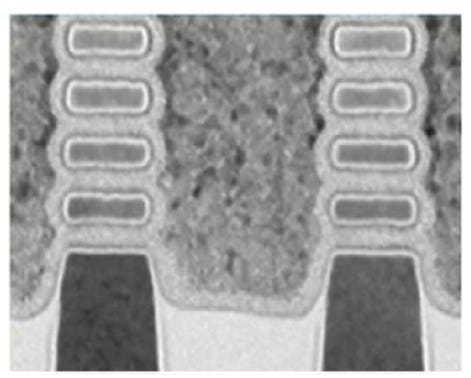
This shift in computing platform also coincides with yet another inflection in transistor architecture. The Gate-all-Around (GAA) or RibbonFET transistor is poised to replace the FinFET. RibbonFET is a natural evolution of the FinFET and delivers enhanced drive current and/or lower capacitance within a given footprint, superior electrostatics, a higher packing density, and the ability to operate at a lower voltage.

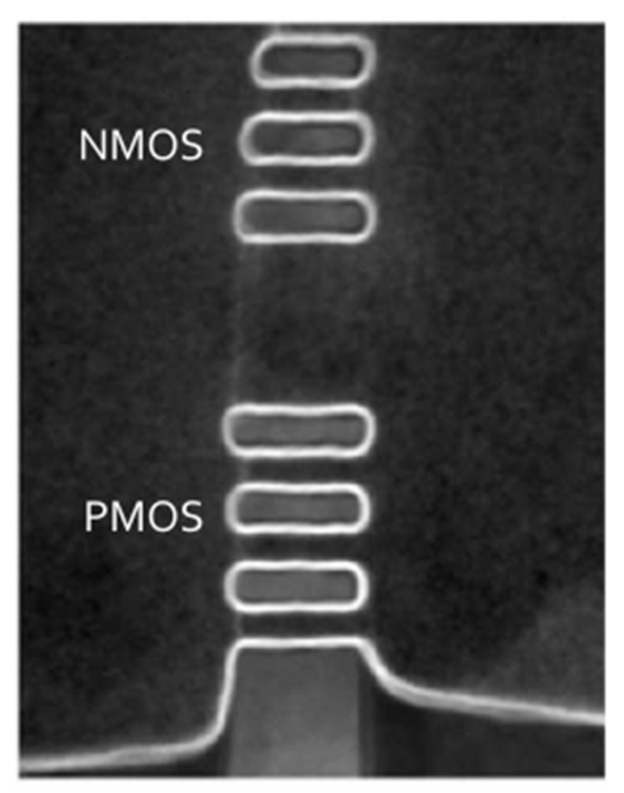
The RibbonFET architecture will likely be succeeded by a stacked-RibbonFET architecture with N and P transistors stacked upon each other to create more compact, monolithic 3D compute units. This architecture can deliver a dramatic (>1.5X) increase in transistor density within a given footprint and has already been demonstrated on silicon by Intel and others.

Beyond stacked silicon RibbonFETs, 2D transition metal chalcogenide (TMD) films are being investigated as channel material for further dimensional scaling, but many issues persist.
Over the last few years, worldwide energy demand for AI computing has been increasing at an unsustainable pace. Furthermore, transitioning to chiplet-based System-in-Package (SiP) designs with 3D stacked chips and hundreds of billions of transistors per package will increase heat dissipation beyond the limits of current best-in-class materials and architectures. Breaking through this impending “Energy Wall” will require coordinated and focused research toward reducing transistor energy consumption and improving heat removal capability.
Call To Action: A New Ultra-Low Energy Transistor
A focused effort is necessary to develop a new transistor capable of operating at ultra-low voltages (Vdd < 300mV) to improve energy efficiency. However, ultra-low Vdd operation can lead to significant performance loss and increased sensitivity to variability, requiring circuit and system solutions to be more resilient to variation and noise. These challenges call for a strong collaboration between the device, circuit, and system communities. Improving transistor performance at ultra-low voltage will require the development of a super-steep sub-threshold slope transistor and the use of high-mobility channel materials.

Potential options for a super-steep sub-threshold slope transistor include Negative Capacitance FET (NC-FET), Ferroelectric FET (FE-FET) and Tunnel FET (TFET), each with unique challenges. Each of these are being actively investigated across industry and academia.

The NC-FET leverages a ferroelectric gate insulator material. Negative differential capacitance in ferroelectrics can amplify changes in surface potential in response to gate voltage, leading to lower sub-threshold slopes and lower equivalent oxide thickness (EOT) (Further reading: Link)
While NC-FET is designed for hysteresis-free operation, FE-FET is hysteretic. As illustrated in the schematic above, the FE-FET relies on ferroelectrics with low coercive voltage to generate an “effective” ultra-steep sub-threshold slope, less than the lowest achievable in silicon transistors (60mV/decade).
Tunnel-FETs have been perennially plagued with low drive current and less-than-projected improvement in sub-threshold slopes.
Given the significant loss in drive current due to low gate overdrive, high-mobility channel materials will also be necessary to boost drive current at ultra-low Vdd. A targeted introduction of high-mobility channel materials such as Germanium, III-Vs, and carbon nanotubes into existing mature silicon substrates is expected to yield rich dividends.

Plenty of Room at the Bottom!
The number of transistors in a microprocessor package will continue to increase substantially over the next ten years. Developing an ultra-low Vdd transistor will help address one of the most significant contributors to AI energy consumption and thermal dissipation concerns in the trillion-transistor era.
At every significant inflection over the last 60 years, when challenges to continued transistor scaling seemed too daunting, technologists across industry and academia forged new paths to enable the arc of exponential progress to continue unabated. There is no reason to believe that this trend will not continue well into the future. There is still plenty of room at the bottom!
The original version of this essay was published as an invited special paper in the proceedings of the recently held 2024 International Electron Devices Meeting (IEDM). This version has been created for a mainstream audience. The views expressed herein are the authors’ own.


Wow Dr. Ghani himself coauthoring this post. Thank you Mr. Transistor and Pushkar 🫡
N2→A16→A14…..