Software 2.0 and the Future of Chip Design
“We took a step back and we said, “What is the implication of this?” Not just for computer vision, but ultimately for how software is done altogether. Recognizing that for the very first time, software is not going to be written – features weren't going to be engineered or created by humans, but somehow automatically extracted out of data, refined out of data to recognize patterns, relationships, and somehow learn the representation of some predictive model — that observation early on caused us to ask the question, "How does this affect the future of software?" How does this affect the future of computer science? How does this affect the future of computing? If the way that you write software is different, then how does it change the way you would design computers? And if the software that's written is written by a computer versus a human, how does that affect the type of computers you would design? We had the good sense of thinking about it — from first principles — the implications for the entire field of computer science and the entire field of industry. Which ultimately led to asking the question, “What about the implications to all the different industries?”
Jensen Huang, describing why NVIDIA moved into the deep learning space, circa 2012 (Link)
Advances in computing have always been enabled by an interplay of hardware and software. Innovations in software drove several generations of progress in hardware and vice-versa. As transistor density doubled every couple of years, computer architecture evolved to take advantage of the additional transistors; and in turn, enabled software to leverage the increased functionality and performance made available by Moore’s Law. Similarly, as computer applications and workloads evolved, software in turn shaped the evolution of computer architecture, making it more efficient for the most predominant workloads. There have been numerous evolutionary advances in computer architecture, chip design methodology and software frameworks that contributed to the computing trajectory over the last five decades.
By contrast, paradigm shifts have been far more infrequent and occurred once in a decade or even longer but drove revolutionary advances across the computing stack and the industry at large. Such paradigm shifts are necessary to consistently raise the design abstraction and enable engineers and architects to manage the growing complexity at every layer of the computing stack. We may be witnessing the early days of the next paradigm shift, referred to as Software 2.0.
This paper articulates how Software 2.0 is likely to drive a new paradigm not only in how we design chips, but in the chip architecture itself. These changes in turn have the potential to alter the established order within the entire semiconductor industry.
Software 2.0 : Humans Train Models
“Neural networks are not just another classifier; they represent the beginning of a fundamental shift in how we develop software. They are Software 2.0. The “classical stack” of Software 1.0 is what we’re all familiar with — it is written in languages such as Python, C++, etc. It consists of explicit instructions to the computer written by a programmer. By writing each line of code, the programmer identifies a specific point in program space with some desirable behavior. In contrast, Software 2.0 is written in much more abstract, human unfriendly language, such as the weights of a neural network. No human is involved in writing this code...”
Andrej Karpathy, Director AI, Tesla (Link)
Starting 2012, deep learning based models began to show dramatic reduction in error rates for image recognition (Link) and natural language processing tasks (Link). By 2014, all the entries in the ImageNet contest used deep learning models and the winning entry had an error rate < 5%, making it better than the average human at image classification from a dataset of thousands of images (Link) ! Since then, there has been a quiet revolution that has been sweeping almost every aspect of our lives. Based on these trends, Andrej Karpathy made an astute observation in 2017 to describe the evolution of software in the age of deep learning and artificial intelligence. He predicted that over time, a large fraction of the codebase we have used for decades will transition from Software 1.0 (code written by humans) to Software 2.0 (code written by a trained neural network model). In this new paradigm, the focus of a human software developer shifts from writing code to creating and curating (labeling) large datasets, which in turn form the input to a model that generates code. Judging by the progress made in the last 5 years, it is fair to say that Andrej has been right, even though we are still a long way from a widescale transition to Software 2.0.
Models Write Code
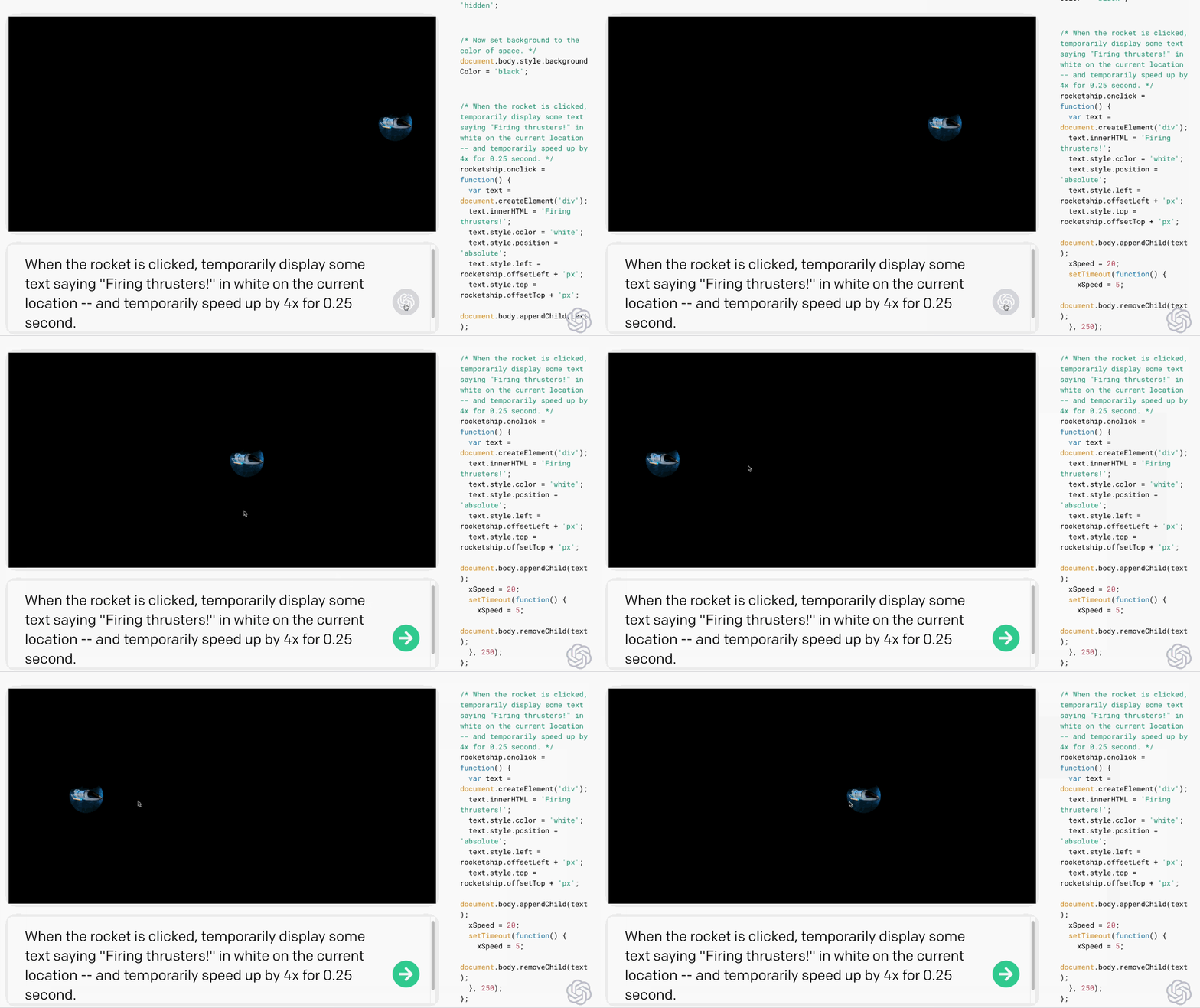
A remarkable visualization of the power of Software 2.0 is this recent public demonstration by OpenAI in which researchers used a model called Codex to create a computer game from scratch using commands in plain English. As seen in the screenshots below, complex instructions written in conversational English were automatically converted to written code by the model in real-time. Codex is a general purpose programming model based on Generative Pre-trained Transformer (GPT-3), a highly sophisticated and vast neural network training model with up to 175B parameters.
Instructions in plain English are instantaneously converted to written code using a deep learning based model (GPT-3) (Link)
One can imagine a data-rich model, trained with chip design input parameters and aware of the relevant reward functions that could one day take simple instructions and translate them to code which could then create simple circuits or IP blocks or even layout entire chips or carry out other complex tasks in the chip design process. As an example, one might be able to abstract away highly complex instructions to plain English as follows:
“Use the 5nm PDK to create a foundational standard cell library, optimized for gate density”
“Create a floorplan using a combination of the following macros and cells”
“Optimize this floorplan to minimize area, while also optimizing for wire length.”
It is important to note that unlike games of Go or Chess, chip design workloads like chip floor planning or chip verification have several orders of magnitude more variables, and hence will require far more compute capability and bigger datasets. In addition, while Go or Chess are games with clear win/lose outcomes, chip design workloads have a gradient of outcomes that can be optimized based on the application of the chip. Nonetheless, results from a variety of companies so far indicate a significant improvement in turnaround time and chip parameters (frequency, power and/or area) when compared to the corresponding traditional human-engineered tasks (Link, Link, Link).
While such a high level of abstraction doesn’t exist yet, at least not in public domain, there is no fundamental reason why it cannot eventually exist. In fact, it represents the ultimate abstraction to hide and manage the exponentially increasing complexity of circuit design with every successive generation of transistor scaling.
Starting the mid-1980s, Intel partnered with researchers at UC Berkeley and led the way in the development and adoption of new Electronic Design Automation (EDA) tools that helped raise the design abstraction and manage the complexity of microprocessor design. This work spawned the entire field of electronic design automation and companies like Synopsys and Cadence, which today are industry leaders were born out of this partnership. Nearly three decades since, it is time for a new paradigm in design automation, this time enabled by deep learning.
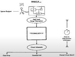
What if a “technology X” could take a language and convert it to circuits? An early sketch illustrating the concept that led to the formation of the company Synopsys and the field of Electronic Design Automation in 1986. (Source : Aart de Geus, Synopsys, HotChips 2021)
Code Designs Chips
The Google DeepMind Challenge Match (Link) in 2016 when the AlphaGo AI beat the world champion Lee Sedol was an inflection point for many other machine learnings (ML) applications – including EDA. ML for EDA is a very active area of research and development today as indicated by a growing number of plenary talks at recent flagship conferences like HotChips, ISSCC and Design Automation Conference (DAC). Every layer of the chip design stack is undergoing a transformation with the infusion of ML. This includes chip architecture, synthesis, place and route, timing, power, test, and verification.
“This incredible growth rate could not be achieved by hiring an exponentially growing number of design engineers. It was fulfilled by adopting new design methodologies and by introducing innovative design automation software at every processor generation. These methodologies and tools always applied principles of raising design abstraction, becoming increasingly precise in terms of circuit and parasitic modeling while simultaneously using ever-increasing levels of hierarchy, regularity, and automatic synthesis. As a rule, whenever a task became too painful to perform using the old methods, a new method and associated tool were conceived for solving the problem. This way, tools and design practices were evolving, always addressing the most labor-intensive task at hand. Naturally, the evolution of tools occurred bottom-up, from layout tools to circuit, logic, and architecture.”
Pat Gelsinger et al, “Coping with the Complexity of Microprocessor Design at Intel”, 2012 (Link)
Synopsys, Cadence, NVIDIA and Google have publicly talked about their efforts in this area (Link), but nearly all major companies are actively working to adopt aspects of this technology. As in all other applications, the companies with the richest datasets will take the lead in this area – and the more data they collect, the wider their moat will become.
Companies like NVIDIA (left) and Google (right) are at the forefront of applying machine learning to chip design (Source : Design Automation Conference 2021)
Chips Designed for Software 2.0
“We are not going to be able to build next-generation chips without AI. And that's kind of a remarkable statement. …Today, we are producing software that gets shipped with all of our AI chips. Without AI, we can't produce software that runs the AI. And in the future, without AI, we wouldn't be able to design the chips that we use to run AI. So, the circular, positive feedback system is about to go into turbocharge. I have every confidence that in the next 10 years, we're going to see even greater advances. Not necessarily at the transistor level, but absolutely at the computation level.”
Jensen Huang, CEO NVIDIA (Link)
Once Software 2.0 becomes the dominant paradigm, not only will it change how we design chips, but it will also affect the architecture of the chips we build. There are several reasons for this as articulated by Andrej Karpathy (Link). Neural networks are computationally homogeneous compared to traditional software and because their instruction sets are relatively small with constant runtimes, it is easier to program them directly on to silicon. Moving software closer to hardware has inherent advantages in performance efficiency. With dramatic improvements in chip design costs and turnaround times enabled by ML, it will become economically viable for more companies to design custom chips (domain specific accelerators) to accelerate specific workloads. Over time, it will also become economical to build a large chip or a collection of chips that are capable of simultaneously supporting multiple classes of trained models, as envisioned by Google Pathways (Link). For these reasons, it is likely that spatial computing (sometimes referred to as graph-based computing) will become the predominant computer architecture in the AI era. Computer architectures that natively process large data sets as a spatially distributed interconnected graph mimic how neural network models are organized and are thus better suited for deep learning workloads. Interestingly, spatially distributed computing also is a good way to mimic how a human brain processes data.
A Paradigm Shift
“Why should a change of paradigm be called a revolution? Political revolutions are inaugurated by a growing sense, often restricted to a segment of the political community, that existing institutions have ceased adequately to meet the problems posed by an environment that they have in part created. In much the same way, scientific revolutions are inaugurated by a growing sense, again often restricted to a narrow subdivision of the scientific community, that an existing paradigm has ceased to function adequately in the exploration of an aspect of nature to which that paradigm itself had previously led the way. In both political and scientific development, the sense of malfunction that can lead to crisis is prerequisite to revolution.”
Thomas S. Kuhn, The Structure of Scientific Revolutions (1961) (Link)
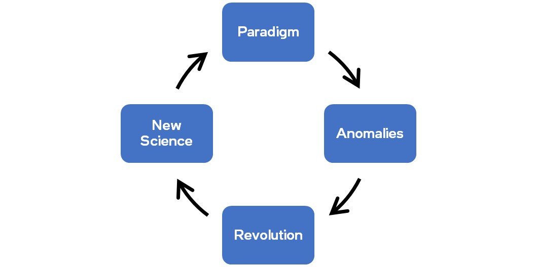
How scientific revolutions happen, adapted from Thomas Kuhn. Image credit : Jim Keller
In the early days of the integrated circuits era, the established paradigm was vertical integration – to manufacture chips, a company had to design them too. And there was no point in designing chips if you didn’t also own the factories to manufacture them – this was viewed as the only way to build semiconductor chips in the early days. Anomalies in this established paradigm showed up when smaller “design houses” began to outsource their manufacturing needs from larger players, primarily because they did not have the means to build and maintain factories to manufacture chips. This culminated in the formation of pure-play foundries like UMC and TSMC – a revolution in hindsight. It took well over two decades for this “new science” of building chips to establish itself as the new, reigning paradigm – what we call the foundry-fabless ecosystem today.
Over time, anomalies are bound to emerge in the reigning foundry-fabless paradigm too – likely leading to another revolution, followed by a “new science” phase when the seeds of the next paradigm will take root.
The established software paradigm since the dawn of computing has been that humans write code and machines execute it to accomplish tasks. We are now beginning to see anomalies in this paradigm where machines can do certain tasks just as well if not better than humans (image/speech recognition and natural language translation are everyday examples). We are also seeing early signs where machines can write code that covers more ground and edge cases than humans are even capable of. As deep learning datasets become richer over time and trained models become more accurate, it will eventually become more common for most code to be written by models, rather than by humans.
There is no reason to believe this will not extend to building silicon chips (across every layer of the stack from initial design-technology co-optimization to architecture, RTL, synthesis, timing, layout, and extending to test and verification). Indeed, we are already seeing numerous anomalies where machine learning can design chips faster than humans and even uncovers design points that lead to better performance, power, area (and hence cost). As transistor density (and resulting chip design complexity) grows exponentially, it is foreseeable that all chip design will eventually be achieved via machine learning. We will initially see this transformation at individual layers (e.g., verification, floor planning, etc.), but over time, this will extend holistically across the EDA stack, when simple commands in English may be able to generate a complete chip layout.
Cloud service providers have the most visibility to a variety of workloads and are best positioned to develop the most comprehensive and efficient training models. We are seeing cloud service providers like Google begin to leverage their scale and insight to build specialized chips for their own workloads. All the EDA tools needed to design chips already exist in the public clouds today (Link). Over time, cloud service providers could just as easily offer machine learning enabled “chip design as a service” on the cloud. This may spur the next chip design revolution; indeed, a paradigm change in how chips will be designed. It is foreseeable that such a revolution will disrupt the established semiconductor world order. Companies that control or own the entire computing stack from chips to the application frameworks and the deep learning models are likely to have an upper hand in such a landscape. Foundries, EDA and IP vendors will shape the new landscape and adapt to it just as much as the cloud service providers and fabless design houses.
These changes will play out over the next decade and perhaps longer as new players and new capabilities emerge, new business and engagement models are defined, and Software 2.0 helps raise the abstraction for chip design.
The views expressed herein are my own.
Many thanks to Jim Keller for enriching discussions that formed the inspiration for this work.


