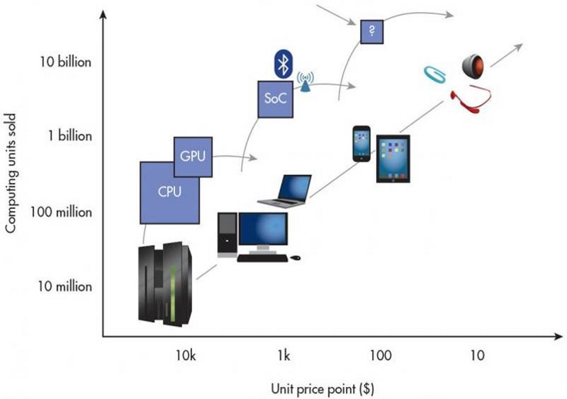
Computing Transitions
A Semiconductor Perspective
A Semiconductor Perspective
Every computing transition has been enabled by a re-architecting of the underlying silicon and software platforms. This post will discuss the specific changes that enabled each wave and posit how the current transition is likely to play out within the global semiconductor industry.
Transition 1: Mainframe to PC ($1000 Price Point)
The first transition occurred in the early 1980s with the development of a very simple single-chip central processing unit (CPU), Intel’s 80286. Operating at just 6 MHz, it continued to be enhanced over three decades through aggressive transistor scaling and a relentless focus on increasing performance (frequency).
Gradually, additional chips such as the graphics processing unit (GPU), memory, and connectivity were added to the system to increase functionality. The CPU-driven hardware ecosystem complemented a mainstream software ecosystem (initially MS-DOS and eventually Windows) and enabled computing on a mass scale (more than 300 million units) with a price point of less than $1000 per unit.
The combination of the CPU and added chips delivered higher performance and more functionality. The CPU and system architecture were designed for performance. Power was a secondary metric. Intel dominated this wave through an aggressive pursuit of Moore’s Law and the predominance of x86 architecture while Microsoft dominated through a virtual monopoly of Windows in the software ecosystem.
Transition 2: PC to Mobile ($100 Price Point)
The consolidation of functionality on a single chip (SoC) enabled the emergence of the smartphone in the late 2000s. The smartphone and tablet deliver desktop-class functionality with a chipset comprising far fewer chips. This wave of computing established the dominance of the SoC and connectivity solutions and delivered even smaller form factors within a much lower power envelope and much lower cost.
The proliferation of mobile computing was also enabled by dramatically cheaper (eventually free) software ecosystems such as iOS (Apple) and Android (Google) that were specifically designed for mobile (SoC) hardware and not for legacy PC (CPU) hardware. Companies like Apple and Qualcomm dominated the early rise of this wave through the aggressive pursuit of chip-level integration, and the SoC emerged the clear winner over the standalone CPU.
Transistor scaling and Moore’s Law helped further enhance the mobile wave by enabling better SoCs and a more compact SoC solution.3 Companies like MediaTek are driving hard to dominate the maturing mobile wave by offering the entire SoC for under $5 and enabling a unit price point of $100 per unit.
Transition 3: Mobile to IoT ($10 Price Point)
Trends suggest that every tenfold increase in unit volume has been enabled by a tenfold reduction in unit price. So what is the right system/chip architecture to enable greater than 30 billion units at a $10 price point? The answer may lie in even higher levels of on-chip integration.
To support the very small form factors and aggressively low power envelopes required for sensor hubs, many system-level functionalities will need to be integrated on a single chip or package, eventually leading to a system-in-package (SiP) or computer-on-chip (CoC). This trend is already evident based on the basic requirements of an IoT chip.
For example, a generic wearable chip may need to deliver a combination of logic computing (CPU), connectivity (radio/Bluetooth/GPS), non-volatile memory (flash), and various analog and mixed-signal functions as well as a variety of sensors. The critical technology metric for such an IoT platform will be its total power envelope, which will need to be as much as 10 times lower than that for a mobile SoC platform.
Semiconductor companies looking to establish leadership in the IoT will need to focus their efforts on functional integration far more than transistor scaling. Several companies are trying to establish early leadership in this space, including a combination of fabless and fab-lite (Qualcomm, Broadcom, Apple, Texas Instruments, STMicroelectronics, NXP Semiconductors), integrated device manufacturers or IDMs (Samsung, Intel), and microelectromechanical-systems or MEMS (STMicroelectronics, Texas Instruments, InvenSense). Foundries too will need to rapidly adapt their transistor technology roadmaps to enable a silicon ecosystem that will enable such integration. With less than a handful of foundries capable of supporting advanced CMOS technology, it is evident that the vast majority of silicon volume needed for IoT applications will be manufactured on legacy silicon technology (28nm or older). The existing foundry ecosystem will need to adapt in order to provide seamless integration of heterogeneous hardware accelerators (logic, connectivity, sensing, memory) in the most compact form factor and at the lowest cost.
In addition to a new silicon architecture and ecosystem, IoT computing will rely on cheap, widely available standard software that will enable the hardware to communicate with each other and to the cloud while allowing an independent and robust developer ecosystem to proliferate. Qualcomm is attempting to take an early lead in this space with AllJoyn while Samsung is promoting its Tizen OS. Google recently released Android Wear for developers in the wearable space. Apple’s HomeKit and HealthKit are attempts to provide developers with platforms around the home and healthcare. Many others are establishing leadership in this emerging market.
The next post will discuss some of the specific requirements for a silicon platform to enable the Internet of Things.


